Séminaire en ligne
Photonic integrated circuits allow for designing computing architectures which process optical signals in analogy to electronic integrated circuits. Therein electrical connections are replaced with photonic waveguides which guide light to desired locations on chip. Through near-field coupling, such waveguides enable interactions with functional materials placed very close to the waveguide surface. This way, photonic circuits which are normally passive in their response are able to display active functionality and thus provide the means to build reconfigurable systems. By integrating phase-change materials nonvolatile components can be devised which allow for implementing hardware mimics of neural tissue. Here I will present our efforts on using such a platform for developing optical non-von Neumann computing devices. In these reconfigurable photonic circuits in-memory computing allows for overcoming separation between memory and central processing unit as a route towards artificial neural networks which operate entirely in the optical domain.
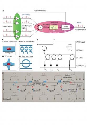
Figure: a, b, Schematic of the network realized in this study, consisting of several pre-synaptic input neurons and one post-synaptic output neuron connected via PCM synapses. The input spikes are weighted using PCM cells and summed up using a WDM multiplexer (MUX). If the integrated power of the post-synaptic spikes surpasses a certain threshold, the PCM cell on the ring resonator switches and an output pulse (neuronal spike) is generated. c, Photonic circuit diagram of an integrated optical neuron with symbol block shown in the inset (top right). Several of these blocks can be connected to larger networks using the wavelength inputs and outputs (see Fig. 5). d, Optical micrograph of three fabricated neurons (B5, D1 and D2), showing four input ports. The four small ring resonators on the left are used to couple light of different wavelengths from the inputs to a single waveguide, which then leads to the PCM cell at the crossing point with the large ring. The triangular structures on the bottom are grating couplers used to couple light onto and off the chip.
OrsayPhotonic integrated circuits allow for designing computing architectures which process optical signals in analogy to electronic integrated circuits. Therein electrical connections are replaced with photonic waveguides which guide light to desired locations on chip. Through near-field coupling, such waveguides enable interactions with functional materials placed very close to the waveguide surface. This way, photonic circuits which are normally passive in their response are able to display active functionality and thus provide the means to build reconfigurable systems. By integrating phase-change materials nonvolatile components can be devised which allow for implementing hardware mimics of neural tissue. Here I will present our efforts on using such a platform for developing optical non-von Neumann computing devices. In these reconfigurable photonic circuits in-memory computing allows for overcoming separation between memory and central processing unit as a route towards artificial neural networks which operate entirely in the optical domain.
Figure: a, b, Schematic of the network realized in this study, consisting of several pre-synaptic input neurons and one post-synaptic output neuron connected via PCM synapses. The input spikes are weighted using PCM cells and summed up using a WDM multiplexer (MUX). If the integrated power of the post-synaptic spikes surpasses a certain threshold, the PCM cell on the ring resonator switches and an output pulse (neuronal spike) is generated. c, Photonic circuit diagram of an integrated optical neuron with symbol block shown in the inset (top right). Several of these blocks can be connected to larger networks using the wavelength inputs and outputs (see Fig. 5). d, Optical micrograph of three fabricated neurons (B5, D1 and D2), showing four input ports. The four small ring resonators on the left are used to couple light of different wavelengths from the inputs to a single waveguide, which then leads to the PCM cell at the crossing point with the large ring. The triangular structures on the bottom are grating couplers used to couple light onto and off the chip.